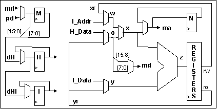
QS5 datapath block diagram
Guided Exploration of two FPGA-based CPU Designs
class #1, May 22, 1999: QS5 Baby RISC
Before attempting to put my 'baby RISC' design onto the XESS board, I had made it as simple as I thought I could: a 16-bit processor with 16-bit address and data busses needing only one memory cycle to access an opcode and/or data. Since I was trying to fit it in as small an FPGA as I could, and was using external SRAM, the ALU only had to be as fast as memory. With 16-bit opcodes it was hard to justify a 3-operand instruction (r1 = r2 + r3) over one with just two (r1 = r1 + r2) because of the reduced number of available operations and the increased size of the decode logic, so a very regular two-operand instruction set was chosen.
However, with just that one cycle to both execute the current opcode and fetch the next one, three different register values (address and 2 ALU inputs) might be needed during each cycle and two might be written back (new address and ALU output). In addition, an address incrementer was needed along with the ALU. With the XESS board's 8-bit data path the constraints changed, and the resulting two cycles needed to access 16-bit values meant some changes could be made.
First, an 8-bit M-register was added to hold the first half of new data and opcodes until the second half arrives, so a 16-bit value could be loaded into H and/or I all at once.
Then, continuing the restriction that 16-bit memory accesses (both data and opcodes) must occur at even addresses, the address incrementer (needed to increment the program counter in parallel with the ALU) was replaced with a combination of the 15-bit N-register, whose low bit is always 1 (to access the next byte of 16-bit values), and use of the ALU during the cycle when the first half of the opcode (or data) is being accessed. This in turn reduced the need for two input and three output values at a time from the register file to just one input and two output values, nicely conforming to the standard dual-port ram blocks available in many FPGAs. The resulting datapath looks like this:
QS5 datapath block diagram
So, with the additional constraint of an 8-bit data bus, the hardware got smaller. What happened to the performance? It didn't quite double the execution time, because the byte load/store opcodes only access one data byte, and the programs didn't change in size at all. Although it hasn't been done yet, decoding of the first half of the opcode might take place while the second half is being fetched, possibly permitting the clock to be faster.
OK, so what do the opcodes look like? The following is from the qasm assembler/disassembler source code file:
\                          QS5 Opcode bit layout (little-endian)
\ OP Class |     High order (odd) byte     |     Low order (even) byte     |
\ ---------+---+---+---+---+---+---+---+---+---+---+---+---+---+---+---+---+
\ template |   iiii/*baa   |   *yyy/uuuu   |f/r|    xxx    |  cc   |  op   |
\ =========+===+===+===+===+===+===+===+===+===+===+===+===+===+===+===+===+
\ call     |           Cell address of machine code routine            | 0 |
\ ---------+---+---+---+---+---+---+---+---+---+---+---+---+---+---+---+---+
\ branch   |  br_  |       distance        | 0 | 1   1   1 | cond  | 0 | 1 |
\          +---+---+---+---+---+---+---+---+---+---+---+---+---+---+---+---+
\ aluop    |     iiii      |    literal    | 0 |    dest   | cond  | 0 | 1 |
\ ---------+---+---+---+---+---+---+---+---+---+---+---+---+---+---+---+---+
\ branch   |  br_  |   *   | * |   source  | 1 | 1   1   1 | cond  | 0 | 1 |
\          +---+---+---+---+---+---+---+---+---+---+---+---+---+---+---+---+
\ aluop    |     iiii      | * |   source  | 1 |    dest   | cond  | 0 | 1 |
\ ---------+---+---+---+---+---+---+---+---+---+---+---+---+---+---+---+---+
\ std      | * | 0 | addr  | * |   source  | 0 | 0   0   0 | cond  | 1 | 1 |
\          +---+---+---+---+---+---+---+---+---+---+---+---+---+---+---+---+
\ out      | * | 1 | addr  | * |   source  | 0 | 0   0   0 | cond  | 1 | 1 |
\          +---+---+---+---+---+---+---+---+---+---+---+---+---+---+---+---+
\ _st      | * | b | stride| * |   source  | 0 |  pointer  | cond  | 1 | 1 |
\ ---------+---+---+---+---+---+---+---+---+---+---+---+---+---+---+---+---+
\ ldd/jpd  | * | 0 | addr  | * |  dest/111 | 1 | 0   0   0 | cond  | 1 | 1 |
\          +---+---+---+---+---+---+---+---+---+---+---+---+---+---+---+---+
\ in       | * | 1 | addr  | * |  dest     | 1 | 0   0   0 | cond  | 1 | 1 |
\          +---+---+---+---+---+---+---+---+---+---+---+---+---+---+---+---+
\ ld_/jp_  | * | b | stride| * |  dest/111 | 1 |  pointer  | cond  | 1 | 1 |
\          +---+---+---+---+---+---+---+---+---+---+---+---+---+---+---+---+
\ ldi/jpi  | * | 0 | 1 | 0 | * |  dest/111 | 1 | 1   1   1 | cond  | 1 | 1 |
\ =========+===+===+===+===+===+===+===+===+===+===+===+===+===+===+===+===+
\     bit#   15  14  13  12  11  10  9   8   7   6   5   4   3   2   1   0

\ notes: - '*' shows an unused opcode bit.
\        - There are many undefined opcodes (i.e., the above table is not a
\           complete list of the possible opcodes, only the decoded ones).
\        - 'ldi' & 'jpi' opcodes are followed by a data word.
\        - The branch distance is measured in cells, starting one cell after
\           the opcode fetched during the current instruction (usually the
\           current address + 4 bytes)
Almost all the instructions are conditional, something I took from HP's PA-RISC machine, eliminating many branches and enabling SIMD multiprocessing.
Bit-0 divides the opcodes into calls (single-level only, like the PPC's Branch-and-Link opcode) and machine opcodes (register-based alu operations, loads, and stores. Each machine instruction, in addition to its regular behavior, is responsible for fetching the next opcode. Normally this is from the program counter, but a single bit allows every machine opcode to simultaneously execute a return.
Bit-1 divides the machine opcodes into alu-opcodes (single machine cycle/two memory cycles, overlapping the fetch/program-counter increment of the next opcode with the specified alu operation) and memory opcodes (two machine cycles/3-4 memory cycles, allowing both a data load/store and an opcode fetch).
Bit-7 further divides each group, separating the alu-opcodes into literal or register operand source and the memory-opcodes into loads and stores. To allow 16-bit 'load immediate' opcodes, the data read occurs before the next opcode fetch. This sequence supports data-address modification after (post-modify) the data is read. In order to provide single-instruction push and pop opcodes, the write had to be able to modify the data address before the data is written. This led me to fetch the next opcode before writing the data (pre-modify).
The assembler was written to recognize code that the students in my UCSC Extension class, used to 'more conventional environments,' would find familiar. What follows, also extracted from the qasm assembler/disassembler file, describes the syntax of the assembly code. The file test.f is an example of assembler source.
(I encourage one of you to create a more 'forth-like' version if you'd like the challenge. Another tool that we might find useful is an interactive software simulator. It would involve extending the disassembler to perform, rather than display, the opcodes.)
\ QASM assembler/disassembler syntax =======================================

\                       nop|ret|nest|exit
\                       call     ADDRESS
\     {CONDITION}       jpi      ADDRESS
\     {CONDITION}       JUMPOP   ADDR|[PTR]
\     {CONDITION}       BRANCH   SOURCE|DISTANCE               DELAYSLOT
\     {CONDITION}       return                                 DELAYSLOT
\     {CONDITION|ret&}  ALUOP    {SOURCE,|SHORT #,} DEST
\     {CONDITION|ret&}  clc|stc|ivc
\     {CONDITION|ret&}  LOADOP   SOURCE, ADDR|[PTR]
\     {CONDITION|ret&}  STOREOP  ADDR|[PTR], DEST
\     {CONDITION|ret&}  ldi      VALUE DEST
\     {CONDITION|ret&}  in       DEST
\     {CONDITION|ret&}  out      SOURCE

\  where braces ({}) enclose optional items, a vertical bar (|) separates
\  alternatives, CAPITALIZED text represents catagories described below,
\  and lower-case text and ALL other punctuation are required.

\     VALUE  Any 16-bit value.

\     SHORT  An unsigned value between 0 and 15.

\  DISTANCE  An unsigned even value between 0 and 126, the number of bytes between
\              the destination address and the opcode address + 4.

\   ADDRESS  Any even (cell aligned) 16-bit address.

\      ADDR  Only with ldd/jpd/std opcodes:    8  10  12  14

\    SOURCE  One of the 8 accessible registers:
\            FL  Flags   (bits: 0000:0000:0000:REQ.ACK.SEND.C)
\            G1  general use                   (ro, rw, rw, rw)
\            G2  general use
\            G3  general use, data stack pointer SP (grows down)
\            G4  general use, return stack pointer RP (grows up)
\            TS  general use, testable
\            RA  general use, return address
\            PC  program counter

\      DEST  One of: FL G1 G2 G3|SP G4|RP TS RA.

\       PTR  One of:    G1 G2 G3|SP G4|RP TS RA.

\ DELAYSLOT  May be any opcode except 'ldi' or 'jdi'. It is always executed,
\            but may have its own condition codes. It should not have 'ret&'.

\ QS5 branch delay-slot issues:
\     The PC (normal) and RA (ret&) values used to fetch the next opcode are their
\ contents at the BEGINNING of the instruction's execution. Branch opcodes modify
\ the PC or RA register in the MIDDLE of the instruction's execution, AFTER the next
\ opcode has been fetched (and AFTER the default update of the PC with the fetch
\ address plus 2).
\     The delay-slot opcode executes with the PC at the branch target address, so:
\     -  'ldi' and 'jpi' have immediate data which will be read from the branch
\        target address instead of the address following the delay-slot opcode.
\     -  'bf' and 'bb' distances are relative to the branch opcode address plus 2.
\     -  'ret&' on a delay-slot opcode overrides the branch target address as the
\        address of its next-opcode fetch.

\ CONDITION  One of the following condition codes:
\              z?  Store results if TS is zero at start of opcode.
\             nz?  Store results if TS is nonzero at start of opcode.

\      ret&  Fetch the next opcode using the value in RA; opcodes
\            without 'ret&' use the value in PC.

\     ALUOP  SOURCE may be omitted when it and DEST are the same register.
\            In the following equations, 's' represents SOURCE or SHORT,
\            'd' is DEST, 'C' is FL[0], and 'c' is the new FL[0].

\            adn     d = d + s                    and     d = d and s
\            sbn     d = d - s                    inv     d = invert s
\            mov     d = 0 + s                    or      d = d or s
\            neg     d = 0 - s                    xor     d = d xor s
\            add   c.d = d + s                    sr      d = C.s[15:1]
\            sub   c.d = d - s                    sl      d = s[14:0].0
\            adc   c.d = d + s + C                rrc   d.c = C.s
\            sbb   c.d = d - s - C                rlc   c.d = s.C

\    BRANCH  to PC + SOURCE:   bf
\            to PC - SOURCE:   bb
\            to SOURCE:        br
\            to PC + DISTANCE: bfi
\            to PC - DISTANCE: bbi
\            to DISTANCE:      bi

\    LOADOP  jump to 16-bit address from memory at ADDR:       jpd
\            jump to 16-bit address from memory at [PTR]:      jp  jp++  jp--
\            jump to  8-bit address from memory at [PTR]:      jpb jpb+  jpb-

\            load 16-bit data from memory at ADDR:             ldd
\            load 16-bit data from memory at [PTR]:            ld  ld++  ld--
\            load  8-bit data from memory at [PTR]:            ldb ldb+  ldb-

\   STOREOP  store 16-bit data to memory at ADDR:              std
\            store 16-bit data to memory at (modified) [PTR]:  st  ++st  --st
\            store  8-bit data to memory at (modified) [PTR]:  stb  +stb  -stb

\ Forth-like assembler control-flow macros are single opcodes. They are branch
\ opcodes, so the range is limited to +65/-63 cells from the next opcode address,
\ and a delay-slot opcode is required where noted. The forward branch around
\ ELSE and REPEAT goes past the delay-slot opcode.

\                     ahead  DELAYSLOT                 begin
\             CONDITION  if  DELAYSLOT      CONDITION  while  DELAYSLOT
\                      else  DELAYSLOT      CONDITION  until  DELAYSLOT
\                      then                           repeat  DELAYSLOT
\                                                      again  DELAYSLOT
Design flow is the term used to describe the tasks that are done to take a design from an idea to working silicon. Every vendor of EDA tools has their own idea of what is involved, and why their tool is required for the best results. After using QuickLogic's 'QuickWorks' tools for three years on small designs, I'm spoiled. Every other environment seems filled with extraneous, time-consuming steps. But most of them have a purpose, even if it's just to fit into a 'legacy' design flow. Here are the steps that we'll go through to create working FPGAs:
logic design
Create the cpu design, in a combination of Verilog and schematic, keeping the device-specific sections separate from the general ones. Here, that means that the distributed register-file and alu modules will need to be done in schematics to fit within the XC4005XL. (My synthesiser reports that it takes 50% of an XC4010XL, but that's probably too much of an XC4005XL for the Xilinx router to complete.)
Also the i/o pad assignment (using a *.ucf file) will be specific to the XESS board.
logic simulation
To make sure that I'm really building what I think I'm building, I do it the Forth way: assemble small, tested modules into the final product. The Xilinx Foundation Express toolset doesn't contain a high-level logic simulator, so they've included a demo package from Simucad. Unfortunately it won't simulate the whole cpu. So we'll need to find another way to do this (or only those of us with full tools wil do this).
What I've done so far (using QuickLogic tools) is to assemble test code (using the Forth metacompiler and qasm assembler) and then disassemble it into a format that can be used by a Verilog Test Fixture, which simulates the environment around the chip. I load the memory image from the disassembler into the simulated RAM, the simulated keyboard input into the test fixture, and start the simulated processor running. The simulator then acts like a logic analyser to show me what's going on.
With the Xilinx tools (which don't simulate the enviornment), we'll have to also use this simulation to generate test vectors for the next two simulation steps.
logic synthesis
This step generates a netlist for the chip design using the gates available on the FPGA we're using. Even schematics can be passed through this step to see if the tool designers can do a better job of mapping your logic to the available gates. Since I rejected Xilinx for this very reason when I first moved from software to hardware design, I'm happy to let them do it. My ALU, in particular, is optimized for the QuickLogic FPGAs (I chose them for two reasons: I could think in terms of their logic blocks, and their demo tools were $99 four years ago.) At this point we'll know whether or not the design will fit in the part. I don't know what we'll find here. A straght-forward port of the qs4 (without using RAM for the register file) led to 135% gate useage on a 4005, 65% on a 4010.
functional simulation
This step is used to verify that the synthesized design produces exactly the same output as the original design. With the QuickLogic tools, I just rerun the Test Bench, comparing it's output to the original output. (Using automated scripts makes this pretty painless.) Here we'll have to apply the test vectors generated above to the chip, verifying that we get the expected outputs. Now we know that the design will work, but we don't know how fast it will be.
place and route
This step puts the gates down and hooks them up, just as if they were parts on a printed circuit board. Compared to the QuickLogic, who guarentees the routability of designs using all of the gates on a chip, Xilinx has very constrained routing resources. They suggest that designs only use 35-75% of the gate resources to ensure routeability. One of the outputs of this step is timing information, which depends more on the routing and fanout than on the logic.
timing simulation
With the timing information from place and route, another simulation is done to check two things: does it go fast enough, and does it have any timing glitches. Assuming good design practices were used, there won't be any of the latter.
bitmap generation and download
Oh boy, lets try it out. Finally we're actually hooked up to the hardware. After the first few times, the preceding steps can be pretty fast--from a few minutes to a couple of hours. Not bad turn-around, really.
There are two ways to get the software loaded into the on-board RAM: XESS supplies a utility which will do it, but the disassembler will have to have another output format added, or the boot mode of the processor can be used.
hardware execution
To get it running, we're going to have to hook up a terminal to the i/o port. Taking advantage of the parallel port, that means more software. The Forth host program will need to be updated for the XESS board, or the chip's i/o modified to meet the requirements of a commercial terminal program
We'll see where we are: my plans are here. The Verilog and Forth code can be found in the directories described here.
I expect that each of you wants to get the cpu's running on your board, but you probably won't have the time or knowledge to do all the work yourself. I encourage you to share out the work and the results. Each of us has different strengths and interests, and together we should be able to do it all. Based on the UCSC classes, I don't expect that the babyrisc chip will be running by next month, so right now I'm planning on talking more about it's instuction set in June.
Then in July we might be ready to start in on the 'twostack' architecture.
 back to introduction
look at source files
ahead to second class
John Rible email: info@sandpipers.com
Updated 6/15/99 ()